

Semiconductor & Microelectronics
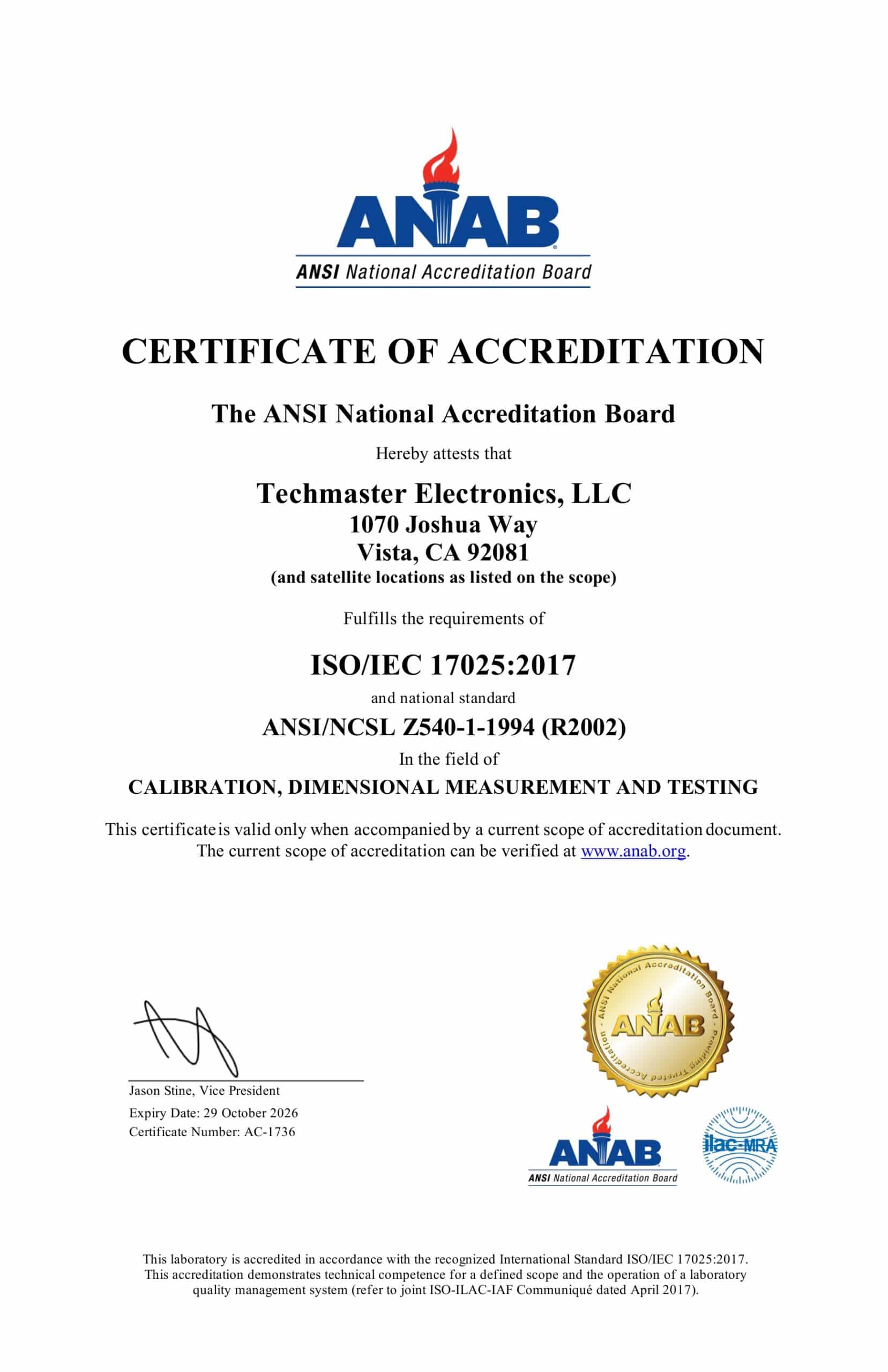
ISO/IEC 17025:2017 accredited calibration, repair, and sales / rentals of RF, electrical, dimensional, and chemistry instruments for SEMI-spec fabs, ATE labs, and wafer-prober test floors · ANAB Certificate AC-1736
Semiconductor & Microelectronics Services
Techmaster Electronics serves wafer fabs, fabless OEMs, IDM customers, photolithography labs, and ATE service bureaus across Silicon Valley, Phoenix, Austin, Boise, RTP, and the Florida Space Coast. From SEMI S2-rated UPW resistivity calibration and wafer-prober SMU verification to mmWave VNA calibration through 110 GHz and dimensional CD-SEM correlation, our 5 US labs deliver fab-floor-ready measurement traceability.
Calibration for Semiconductor
Top calibration disciplines for semiconductor fabs, photolithography labs, and ATE customers.
Repair for Semiconductor
Factory-trained repair for fab-floor instruments, wafer-test heads, and parametric analyzers.
Sales & Rentals for Semiconductor
Authorized partner sales and project rentals for semiconductor R&D and fab production.
Compliance & Industry Standards
Techmaster cal certificates satisfy the audit requirements of every major semiconductor quality framework:
UUTs We Calibrate
Comprehensive list of Unit-Under-Test (UUT) instruments customers in this industry typically send to Techmaster for ISO/IEC 17025 accredited calibration. Click any linked item for a deep-dive article on its calibration procedure, uncertainty budget, and typical failure modes.
Wafer Test & Parametric UUT
- Source Measure Unit
- Picoammeter
- Electrometer
- Power Supply
- Power Analyzer
- Multimeter
- Digital Panel Meter
- Resistance Meter
- Capacitance Meter
- Portable Capacitance Meter
- Inductance Meter
- Milliohm Meter
RF / mmWave UUT
- Spectrum Analyzer
- Vector Network Analyzer
- Signal Generator
- Vector Signal Generator
- Phase Noise Analyzer
- Noise Figure Analyzer
- Power Meter
- Power Sensor
- Frequency Counter
- Pulse Generator
- Mixed Signal Oscilloscope
Chemistry / UPW UUT
- pH Meter
- Conductivity Meter
- TDS Meter
- Resistivity Meter
- Dissolved Oxygen Meter
- TOC Analyzer
- Titrator
- Hot Plate Stirrer
- Stirrer Plate
Dimensional (CD & Wafer Metrology) UUT
- Caliper
- Digital Caliper
- Micrometer
- Depth Micrometer
- Dial Indicator
- Bore Gage
- Gauge Block
- Pin Gauge
- Optical Comparator
- CMM
- Microfinish Comparator
- Surface Plate
ESD & Cleanroom UUT
EMC / EMI (Equipment Compliance) UUT
- EMI Receiver
- LISN
- RF Antenna
- ESD Simulator
- EFT Generator
Need mmWave VNA cal through 110 GHz, fab-floor UPW resistivity, or wafer-prober SMU verification?
Our semiconductor specialists handle mmWave VNA calibration through 110 GHz, on-site UPW resistivity audits, SEMI S2 / S8 equipment compliance, parametric-analyzer refurbishment, and CD-SEM correlation standards.
Frequently Asked Questions
Common questions about Techmaster semiconductor and microelectronics test equipment services.
Can you calibrate mmWave VNAs through 110 GHz?
Do you support SEMI S2 / S8 equipment safety audits?
Can you calibrate parametric analyzers and SMUs?
Can you support on-site UPW resistivity audits?
Which Techmaster locations serve semiconductor customers?
Ready for a semiconductor fab calibration proposal?
Send us your instrument list, target SEMI / JEDEC standards, and fab schedule. We will respond within one business day with a scope proposal aligned to your tool group requirements.
